

FPGA Implementation of TIC TAC TOE using Spartan3 FPGA Image Processing kit
Call for Price
This design accomplished Tic-Tac-Toe game on Spartan3 FPGA Image Processing kit in VHDL. Firstly, designing the circuits and wiring on experiment board.
Package Includes:
-
Spartan3 project board
-
Demo Video
-
Abstract
-
Reference Paper
-
source code
-
!!! Online Support !!!
Description
Abstract
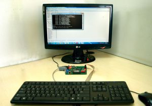
This design accomplished Tic-Tac-Toe game on Spartan3 FPGA Image Processing kit in VHDL. Firstly, designing the circuits and wiring on experiment board. Secondly, designing the algorithm and programming it in VHDL. Thirdly, synthesizing it in Xilinx Synthesis tool and then implementing it in Xilinx ISE developing suite. Finally download it onto FPGA to run it. This design allows two players to play Tic-Tac-Toe game on the experiment board. The user plays the game from the keyboard. He uses the arrows to move a square on a 3×3 grid on the VGA display. The Xs and 0s are placed by pressing the space bar. The user can move a switch to choose the game mode. He can play against another player or alone against the design. When playing alone, after a X is placed the position of the 0 is returned but not yet shown on the display. Only after another key is pressed the 0 appears on the grid. When the game ends (X or 0 wins or draw game) the marks are automatically erased from the grid and the score is incremented on the seven-segment LED display.
Demonstration Video
Tool required
Software:
- xilinx ISE 11.1i
Language:
- VHDL
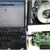
Hardware:
- Spartan3 FPGA Image Processing kit
- VGA Monitor
- PS/2 Keyboard
Block Diagram for TIC TAC TOE using Spartan3 FPGA Image Processing kit

Introduction
Tic-Tac-Toe was tested on Spartan3 FPGA Image Processing kit with a PS2 keyboard and a VGA display. The design of the Tic-Tac-Toe circuit is quite simple. It has 4 inputs and 7 outputs. CLK is the system clock. The keyboard uses a two-wire serial bus including clock and data (KC and KD) to communicate with the host device. Then there is the selection SEL which is connected to a switch from the board. It selects between tow playing modes: player1 vs. player2 or player vs. the board. If player vs. board is selected the circuit picks the next move.
The outputs go to the VGA display and the seven-segment LED display of the board. The board contains a modular 4-digit, common anode seven-segment LED display. In a common anode display, the seven cathodes of the LEDs forming each digit are connected to four common circuit nodes labelled AN0 through AN3. The cathodes of similar segments on all four displays are also connected together into seven common circuit nodes labelled SSEG0 through SSEG6. The five standard VGA signals Red (RED), Green (GRN), Blue (BLU), Horizontal Sync (HS), and Vertical Sync (VS) are routed directly to the VGA connector.

Signal Mode Description
| CLK | Clock input | Main clock input |
| KD | PS2 data input | The keyboard sends data to the host only when both   the data and clock lines are high (or idle). |
| KC | PS2 clock input | The keyboard sends data to the host only when both   the data and clock lines are high (or idle). |
| SEL | Switch input | Selects game mode |
| AN | Output – 7-seg signal | Used to put the score on the seven-segment LED display |
| SSEG | Output – 7-seg signal | Used to put the score on the seven-segment LED display |
| RED | Output – VGA signal | |
| GRN | Output – VGA signal | |
| BLU | Output – VGA signal | |
| HS | Output – VGA signal | |
| VS | Output – VGA signal |
Hardware implementation of TIC TAC TOE game using FPGA
1)Power connection ,VGA and PS2 connection to the FPGA kit
Power connection ,VGA and PS2 connection to the FPGA kit")
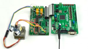
2)JTAG connection with the FPGA kit.
JTAG connection with the FPGA kit.")
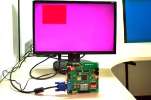
3) VGA output of the TIC TAC TOE game
 VGA output of the TIC TAC TOE game")
 VGA output of the TIC TAC TOE game")
Conclusion
TIC TAC TOE Game was successfully implemented in Spartan3 FPGA Image Processing kit with PS/2 keyboard and VGA monitor interface.
Additional information
| Weight | 1.000000 kg |
|---|
Reviews
There are no reviews yet.