

User Manual for TMS320F2812 Development Kit
Introduction
PRIMER-TMS320F2812 Kit, is proposed to smooth the progress of developing and debugging of various designs encompassing of High speed 16-bit Architecture from Texas Instrument. The board supports most of the TI components devices and some peripheral options in the Code Composer Studio v4. It integrates on board LEDs, UART, Relays, LCD Display, PWM Motor CONTROL Interface, ADC, SPI DAC, SPI EEPROM and CAN on board XDS100 USB V1 EMULATOR.
Packages
☞PRIMER-TMS320F2812 Kit
☞USB CABLE
☞Serial Port Cable
☞5V Adapter
☞Printed User Manual
☞DVD contains Software (Programmers, IDE) & Example Programs
Specifications
MCU
☞Texas Instrument TMS320, TMS320F2812 ( 16 Bit DSC )
Memory
☞Flash Devices: Up to 128K x 16 Flash (Four 8K x 16 and Six 16K x 16 Sectors)
☞ROM Devices: Up to 128K x 16 ROM 1K x 16 OTP ROM
☞L0 and L1: 2 Blocks of 4K x 16 Each Single-Access RAM (SARAM)
☞H0: 1 Block of 8K x 16 SARAM
☞M0 and M1: 2 Blocks of 1K x 16 Each SARAM
Clock
☞25MHz crystal
☞(125MHz CPU clock)
On-Board Peripherals
☞On Board XDS100 USB Emulator V1
☞8 Nos. LEDs
☞4 Nos. Digital Input(Slide Switch)
☞8 Push Switch
☞2X16 Character LCD with back Light
☞4 Nos. Analog Input (Potentiometer)
☞256k SPI EEPROM
☞12 bit SPI DAC
☞CAN Interface to study
☞1 Nos. of SPDT Relay
☞UART(RS232) interface
☞Buzzer (Alarm)
☞Boot Mode Options
Power
☞5V DC- Adaptor,Power from USB (+5V) (+3.3V, 800mA)
Connectors
☞1 Nos. 50 Pin Address & Data lines connector
☞3 Nos.20 Pin Port Connectors
☞External SPI Connectors
☞JTAG (Programming/ Debugging)
☞RS232 Connector (Serial Port)
☞20 – PIN Expansion Connector
☞External Analog Input Connector
☞External Relay Input Connector
☞Power Connector
☞USB Connector
☞SPI DAC Connector
☞CAN Connector
General Block Diagram
TMS320F2812 Processor Features
☞16-bit Digital Signal Controller CPU from TEXAS Instruments in a 176 pin LQFP package.
☞High-Performance Static CMOS Technology – 150 MHz (6.67-ns Cycle Time) – 150 MHz (6.67-ns Cycle Time) 1.9-V Core @150 MHz, 3.3-V I/O) Design
☞JTAG Boundary Scan Support
☞High-Performance 32-Bit CPU ( TMS320C28x™) – 16 x 16 and 32 x 32 MAC Operations – 16 x 16 Dual MAC – Harvard Bus Architecture – Atomic Operations – Fast Interrupt Response and Processing – Unified Memory Programming Model – 4M Linear Program/Data Address Reach – Code-Efficient (in C/C++ and Assembly) – TMS320F24x/LF240x Processor Source Code Compatible
☞On-Chip Memory – Flash Devices: Up to 128K x 16 Flash (Four 8K x 16 and Six 16K x 16 Sectors) – ROM Devices: Up to 128K x 16 ROM – 1K x 16 OTP ROM – L0 and L1: 2 Blocks of 4K x 16 Each Single-Access RAM (SARAM) – 0: 1 Block of 8K x 16 SARAM – M0 and M1: 2 Blocks of 1K x 16 Each SARAM
☞Boot ROM (4K x 16) – With Software Boot Modes – Standard Math Tables
☞External Interface (2812) – Over 1M x 16 Total Memory – Programmable Wait States – Programmable Read/Write Strobe Timing – Three Individual Chip Selects
☞Clock and System Control – Dynamic PLL Ratio Changes Supported – On-Chip Oscillator – Watchdog Timer Module
☞Three External Interrupts
☞Peripheral Interrupt Expansion (PIE) Block That Supports 45 Peripheral Interrupts
☞Three 32-Bit CPU-Timers
☞128-Bit Security Key/Lock – Protects Flash/ROM/OTP and L0/L1 SARAM – Prevents Firmware Reverse-Engineering
☞Motor Control Peripherals – Two Event Managers (EVA, EVB) – Compatible to 240xA Devices
☞Serial Port Peripherals – Serial Peripheral Interface (SPI) – Two Serial Communications Interfaces (SCIs), Standard UART – Enhanced Controller Area Network (eCAN) – Multichannel Buffered Serial Port (McBSP)
☞12-Bit ADC, 16 Channels – 2 x 8 Channel Input Multiplexer – Two Sample-and-Hold – Single/Simultaneous Conversions – Fast Conversion Rate: 80 ns/12.5 MSPS
☞Up to 56 General-Purpose I/O (GPIO) Pins
☞Advanced Emulation Features – Analysis and Breakpoint Functions – Real-Time Debug via Hardware
☞Real-Time Debug via Hardware – ANSI C/C++ Compiler/Assembler/Linker – Code Composer Studio IDE – DSP/BIOS – JTAG Scan Controllers
☞Low-Power Modes and Power Savings – IDLE, STANDBY, HALT Modes Supported – Disable Individual Peripheral Clocks
Connector Details
Expansion Connectors
SPI Connector
ADC Connector
Address and Data Bus Connector
3.5 JTAG Connector
3.6 Jumper Details
| Power supply J2 |  | Adapter (+5V) usb cable(+5V) |
| XMP/MC J7 | | Micro controller mode select Micro processor mode select |
| PLLDIS J6 | | PLL Disable PLL Enable |
| SPI EEPROM J15 | | No connection Chip select – GPIOG5 |
| SPI EEPROM J16 | WP | Write Protect pin for SPI EEPROM Don’t place jumper. |
| SPI DAC J18 | | Chip Select – SPI Enable pin Chip Select – GPIOG4 pin |
| PORT A J20 | | 3.3V select for expansion connector 5V select for expansion connector |
| PORT B J21 | | 3.3V select for expansion connector 5V select for expansion connector |
| PORTD/E/G J22 | | 3.3V select for expansion connector 5V select for expansion connector |
3.7 Test point Details
The following test points are used to check or test the boards,
☞TP1 – ADCREFIN
☞TP2 – READ/WRITE
☞TP3 – 5V
☞TP4 – 3.3V
☞TP5 – 1.8V
☞TP6 – GROUND
☞TP7 – RESET
☞TP8 – XCLK IN
☞TP9 – XCLC OUT
☞TP10 – CLKOUT
3.8 Boot mode Selection
The Boot ROM is factory-programmed with boot-loading software. The Boot ROM program executes after device reset and checks several GPIO pins to determine which boot mode to enter. For example, the user can select to execute code already present in the internal Flash or download new software to internal RAM through one of several serial ports. Other boot modes exist as well.
|
BOOT MODE SELECTED |
GPIOF4 (SCITXDA) |
GPIOF12 (MXDA) |
GPIOF3 (SPISTEA) |
GPIOF2 (SPICLK) |
|
GPIO PU status(3) |
PU |
NO PU |
NO PU |
NO PU |
|
Jump to Flash/ROM address 0x3F 7FF6. |
1 |
x |
x |
x |
|
Call SPI_Boot to load from an external serial SPI EEPROM |
0 |
1 |
x |
x |
|
Call SCI_Boot to load from SCI-A |
0 |
0 |
1 |
1 |
|
Jump to H0 SARAM address 0x3F 8000 |
0 |
0 |
1 |
0 |
|
Jump to OTP address 0x3D 7800 |
0 |
0 |
0 |
1 |
|
Call Parallel_Boot to load from GPIO Port B |
0 |
0 |
0 |
0 |
Note: PU = pin has an internal pullup.
No PU = pin does not have an internal pullup. 1 = high logic (3.3v) 0 = low logic (0v) x = Either High / Low Logic
Power Supply
The external power can be DC, with a voltage 5V/1A output at 230V AC input. The TMS320F2812 board produces 3.3V were using an ADP3339 voltage regulator, This Voltage providing supply to the Controller & related peripherals. LM1117 voltage regulator will produce the 1.8V and used for core voltage of Digital Signal Controller. Here, USB meant for power supply as well as XDS100 USB V1 Emulator. Separate power source select Jumper available.
|
PWR SW1 |
ON OFF |
On/Off Switch (SW1) for controlling power to the board.
Note: Refer Jumper table for power source select
On-board Peripherals
This Development kit comes with following interfacing options
☞On Board XDS100 USB V1 Emulator
☞8 Number LEDs
☞4 Number Digital Input(Slide Switch)
☞8 Push Switch Digital Input
☞16×2 Character LCD with back Light
☞4 Number Analog Input (Potentiometer)
☞256k SPI EEPROM
☞12 bit SPI DAC
☞CAN Interface to study
☞1 Number of SPDT Relay
☞UART(RS232) interface
☞Buzzer (Alarm)
☞Boot Mode Options (SARAM/FLASH)
General Procedure to Work F2812
1. Open Code Composer Studio v4.
2. In Workspace Launcher.
☞BROWSE → Select the project location and make one new folder, MAKE NEW FOLDER → Type the Workspace name, OK → OK.
3. FILE → NEW → CCS PROJECT
☞Project name: Type your project name.
☞Tick use default location. →NEXT
☞Project type: C2000.
☞Tick Debug and Release. →NEXT → NEXT.
☞Output type: Executable.
☞Device Variant: generic C28xx Device and TMS320F2812.
☞Device Endianness : little
☞Code Generation Tools: TI v5.2.3.
☞Run time support library: automatic.
☞Target content: none. →FINISH
4. FILE → NEW → SOURCE FILE
☞Source file: Type your projectname.c (.c extension is must).
☞Type the program.
☞FILE → SAVE.
Paste the following library files in Project location.
☞DSP281x_CpuTimers.c
☞DSP281x_DefaultIsr.c
☞DSP281x_GlobalVariableDefs.c
☞DSP281x_PieCtrl.c
☞DSP281x_PieVect.c
Paste the following Linker file in the project location.
☞DSP281x_Headers_nonBIOS.cmd
☞F2812_EzDSP_RAM_lnk.cmd
Note: Those c files and linker files are available at cd.
5. PROJECT → PROPERTIES → C/C++ BUILD → BASIC OPTION
☞Target processor version(–silicon version, -mv) : 28
- IN C/C++ BUILD, → INCLUDE OPTIONS (Add dir to #include search path (–include path,-I)) select this add icon and add the following two path by individually. “${XDAIS_CG_ROOT}/packages/ti/xdais” “C:/tidcs/c28/DSP281x/v120/DSP281x_headers/include☞IN C/C++ BUILD, →c2000 linker ->file search path (Add dir to #include search path(–include path,-I)) select this add icon and add the following three path by individually. “rts2800_ml.lib” “${PROJECT_ROOT}” “C:\Program Files\Texas Instruments\ccsv4\tools\compiler\c2000\lib”FILE → NEW → TARGET CONFIGURATION FILE7. In C/C++ Project window, Right click the project →REBUILD PROJECT.8. Connections:TARGET → DEBUG ACTIVE PROJECT.(Then see out at corresponding place after run)☞file name: projectname. ccxml (.ccxml extension is must)☞Connection: Texas Instrument XDS100 v1 USB Emulator.☞Device: TMS320C2812. → SAVE.☞Connect the usb cable, PC to KIT.☞Connect the 5v adapter and Power on the kit.Code Composer StudioIntroduction of Code Composer StudioCode Composer Studio Integrated Design Environment for the C2000 Family of Texas Instruments Digital Signal Processors. Simply, Code Composer Studio is the environment for project development for all tools needed to build an application for the C2000-Family.The objective of this module is to understand the basic functions of the Code Composer Studio v4, how to create and debug a project in CCS v4 for TMS320F2812 Kit/F28335 kit. This following section will introduces some of the basic features and functions in Code Composer Studio so you can create and build simple projects. Experienced users can proceed to the following sections for more in-depth explanations of Code Composer Studio’s various features.Finally, you will able to work the TYRO-TMS320F2812/TMS320F28335/TMS320F28069 kit with CCS v4Launching The Code Composer Studio V4Click this icon shown on your desktop. A prompt will appear asking for a workspace location. To launch Code Composer Studio IDE for the first time, configure Code Composer Studio for a fixed workspace location.Setting The Workspace LocationTo create a workspace location using standard configuration file:1. Double-click the Setup CCStudio icon on desktop.
 The workspace launcher dialog box appears.Note: Be sure that workspace location is empty for a fresh project2. Tick the use this as the default and do not ask again (Optional).Note: Again to get the workspace launcher at startup. open ccs go to window – preference – general – startup and shutdown – tick “prompt for workspace on startup”.3. Click ok.4. The empty workspace editor will open.
Create a New Project
To create a project, follow these steps:
1. Launch Code Composer Studio. See Chapter 2
2. From the CCStudio File menu, choose New – CCS Project.
New CCS Project dialog box appears.
3. In the Project Name field, type the project name & click Next.
5. In the Project type field, Select C2000.
6. Tick Debug and Release in configuration box. Click Next.
7. Then also, Click Next.
8. In output Type, select the Executable.
9. In Device Variant , Choose TMS320C28XX & TMS320F2812 Kit.
10. Click Finish. Code Composer Studio creates a project file called practice.pjt. This file stores your project settings and references the various files used by your project.
11. From the CCStudio C/C++ Projects, Right click the led [ Active – Debug ] New – Source File.
12. In the source file field, Type the source file name with extension. (led.c)
13. Click Finish.
14. Type the program in led.c editorwindow then , File – Save.
Add a Files to Project
After Creating the project and source file we must add some addition files to our project. These addition files may vary depend upon the projects which we used.
Create/add new source files to your project by right-clicking on the project in the “C/C++ Projects”
1. From the CCStudio C/C++ Projects, Right click the led [ Active – Debug ] Select the Add files to project or you can directly paste the needed files to the project location, if you paste these files in project location then no need to proceed Add files to project step.
a. Paste the following library C files in project location.
☞DSP281x_CpuTimers.c
☞DSP281x_DefaultIsr.c
☞DSP281x_GlobalVariableDefs.c
☞DSP281x_PieCtrl.c
☞DSP281x_PieVect.c
b. Paste the following Linker file in the project location.
☞DSP281x_Headers_nonBIOS.cmd
☞F2812_EzDSP_RAM_lnk.cmd
Note: Those c files and linker files are available at DVD.
2. Then browse and select all the needed files.
3. Click Open. The selected all the files are added to your project.
Create a Target Configuration File
1. From the CCStudio C/C++ Projects, Right click the led [ Active – Debug ] New – Source File.
2. New Target Configuration dialog appears. Then Click Finish
NewTargetConfiguration.ccxml will open, This will help to communicate between hardware and softeware. While connecting the hardware to the software the target configuration file will run. If any initialize needed we can add gel file additionally in the target configuration.
3. In General setup, there are more connection available to choose. Accorcding to our board, we have to choose XDS 100 USB emulator version 1 and TMS320F2812( Target Device ).
4. Tick the TMS320F2812 & Click Save.
Build a Project
Before Building the project we must modify project properties , add the include files and path according to our usage.
1. From the CCStudio C/C++ Projects, Right click the led [ Active – Debug ] – Properties.
2. In C/C++ Build, go to C2000 compiler
☞Include Options (Add dir to #include search path(–include_path,-I)) select this add icon ![]() and add the following three path by indivdually.“${XDAIS_CG_ROOT}/packages/ti/xdais” “C:/tidcs/c28/DSP281x/v120/DSP281x_headers /include”
and add the following three path by indivdually.“${XDAIS_CG_ROOT}/packages/ti/xdais” “C:/tidcs/c28/DSP281x/v120/DSP281x_headers /include”
3. IN C/C++ Build, go to c2000 linker
☞Basic option – stack size – 0x400.
☞Include library file or command file as input (–library,-I)“rts2800_ml.lib”
☞file search path (Add to library search path(–include_path,-i)) select this add icon ![]() and add the following three path by indivdually. “${PROJECT_ROOT}” “C:\Program Files\Texas Instruments\ccsv4\tools\compiler\c2000\lib”
and add the following three path by indivdually. “${PROJECT_ROOT}” “C:\Program Files\Texas Instruments\ccsv4\tools\compiler\c2000\lib”
4. From the CCStudio C/C++ Projects, Right click the led [ Active – Debug ] – Build Project or Rebuild Project.
Note: Once the project is successfully build you will get 0 Errors. If Errors arise check the code and project properties then rebuild the project.
Run a project
To run a project ,
1. Target – Debug Active Project.
Note: at this step, Target will connect, gel file will run, led.out will load to target then finally Keep the cursor at main() of program to start execute.
2. This is Debug workspace., at this we can debug a code using breakpoints, single stepping, watch window, memory etc..,
3. Target – Run.
For led code, check the output at on board. The Leds is will on and off with few delay.
4. Target – Halt.
5. Target – Terminate all.
Again, the ccs will return to edit workspace from debug workspce.
6. Close the Code composer studio.
Console Window
The Output window is located at the bottom of the screen by default. By default, the printf function displays in console window, showing information such as the contents of Stdout and the build log.
Help
Code Composer Studio provides many help tools through the Help menu. Select Help Contents to search by contents. Select Help Tutorial to access tutorials to guide you through the Code Composer Studio development process.
Select Help Web Resources to obtain the most current help topics and other guidance. User manuals are PDF files that provide information on specific features or processes. You can access updates and a number of optional plug-ins through Help Update Advisor.
EXAMPLE PROGRAMS ON TMS320 KIT(TMS320F2812 Kit)
Example 1: Running an LED
Example 2: Push Button and Led
Example 3: Switch and Led
Example 4: Buzzer
Example 5: Relay
Example 6: LCD
Example 7: UART
Example 8: ADC
Example 9: PWMA
Example 10: PWMB
Example 11: SPI EEPROM AT25HP256
Example 12: SPI DAC MCP4921
Example 1: Running an LED
Project Description:
This example code shows the indication of LED On/Off. By driving a High logic to output port pin illuminate an LED. Driving High and Low logic with delay LED turns on and off alternatively.
Hardware Connections:
| HARDWARE PIN OUT | CONNECTIONS | OUTPUT | |
| D2 | GPIOF7 | Select the 2nd Switch SW11 to Enable Led | LED’s will be Turned ON and OFF at regular interval. |
| D3 | GPIOF8 | ||
| D4 | GPIOF9 | ||
| D5 | GPIOF10 | ||
| D6 | GPIOF11 | ||
| D7 | GPIOF12 | ||
| D8 | GPIOF13 | ||
| D9 | GPIOF14 |
Source Code:
Running LED on TMS320F2812 Kit
Verify Output:
The Led Will On and Off alternatively.
Example 2: Push Button and Led
Project Description:
This example code shows the indication of LED according to push button state. By reading a push button state from PORTA and PORTB and writing the corresponding value to PORTF illuminates an LED.
Hardware Connections:
| HARDWARE PIN OUT | CONNECTIONS | OUTPUT | |
| D2 | GPIOF7 | Select the 2nd Switch SW11 to Enable Led | LED’s will be Turned OFF according to switch state. |
| D3 | GPIOF8 | ||
| D4 | GPIOF9 | ||
| D5 | GPIOF10 | ||
| D6 | GPIOF11 | ||
| D7 | GPIOF12 | ||
| D8 | GPIOF13 | ||
| D9 | GPIOF14 | ||
| SW3 | GPIOA11 | – | |
| SW4 | GPIOA12 | ||
| SW5 | GPIOA13 | ||
| SW6 | GPIOA14 | ||
| SW7 | GPIOB11 | ||
| SW8 | GPIOB12 | ||
| SW9 | GPIOB13 | ||
| SW10 | GPIOB14 |
Source Code:
#include "DSP281x_Device.h"

#define LED1 GpioDataRegs.GPFDAT.bit.GPIOF7

#define LED2 GpioDataRegs.GPFDAT.bit.GPIOF8

#define LED3 GpioDataRegs.GPFDAT.bit.GPIOF9

#define LED4 GpioDataRegs.GPFDAT.bit.GPIOF10

#define LED5 GpioDataRegs.GPFDAT.bit.GPIOF11

#define LED6 GpioDataRegs.GPFDAT.bit.GPIOF12

#define LED7 GpioDataRegs.GPFDAT.bit.GPIOF13

#define LED8 GpioDataRegs.GPFDAT.bit.GPIOF14

// Prototype statements for functions found within this file. void delay_loop(long);

void Gpio_select(void);

void InitSystem(void);

void main(void)

{

unsigned int i;

unsigned int LED[8]= {0x0001,0x0002,0x0004,0x0008, 0x0010,0x0020,0x0040,0x0080};

InitSystem();

// Initialize the DSP's core Registers Gpio_select();

// Setup the GPIO Multiplex Registers while(1)

{

for(i=0;i<14;i++)

{

if(i<7) GpioDataRegs.GPFDAT.all = ((LED[i])<<7);

else GpioDataRegs.GPFDAT.all = ((LED[14-i])<<7);

delay_loop(10000000);

}

}

}

void delay_loop(long end)

{

long i;

for (i = 0; i < end; i++);

}

void Gpio_select(void)

{

EALLOW; GpioMuxRegs.GPFMUX.all = 0x0;

GpioMuxRegs.GPFDIR.all = 0x7F80;

// GPIO PORT as input EDIS;

}

void InitSystem(void)

{

EALLOW;

SysCtrlRegs.WDCR= 0x0068;

// Setup the watchdog SysCtrlRegs.SCSR = 0;

// Watchdog generates a RESET SysCtrlRegs.PLLCR.bit.DIV = 10;

// Setup the Clock PLL to Xly by 5 SysCtrlRegs.HISPCP.all = 0x1;

// HSPCP Prescaler to divide by 2 SysCtrlRegs.LOSPCP.all = 0x2;

// LSPCP Prescaler to divide by 4

// Peripheral clock enables set for the selected peripherals. SysCtrlRegs.PCLKCR.bit.EVAENCLK=0;

SysCtrlRegs.PCLKCR.bit.EVBENCLK=0;

SysCtrlRegs.PCLKCR.bit.SCIAENCLK=0;

SysCtrlRegs.PCLKCR.bit.SCIBENCLK=0;

SysCtrlRegs.PCLKCR.bit.MCBSPENCLK=0;

SysCtrlRegs.PCLKCR.bit.SPIENCLK=0;

SysCtrlRegs.PCLKCR.bit.ECANENCLK=0;

SysCtrlRegs.PCLKCR.bit.ADCENCLK=0;

EDIS;

}
Push Button and Led on TMS320F2812 Kit
#include "DSP281x_Device.h"

#define SW1 GpioDataRegs.GPDDAT.bit.GPIOD0

#defin SW2 GpioDataRegs.GPDDAT.bit.GPIOD1

#defin SW3 GpioDataRegs.GPDDAT.bit.GPIOD5

#defin SW4 GpioDataRegs.GPDDAT.bit.GPIOD6

#defin LED1 GpioDataRegs.GPFDAT.bit.GPIOF7

#defin LED2 GpioDataRegs.GPFDAT.bit.GPIOF8

#defin LED3 GpioDataRegs.GPFDAT.bit.GPIOF9

#defin LED4 GpioDataRegs.GPFDAT.bit.GPIOF10

#defin LED5 GpioDataRegs.GPFDAT.bit.GPIOF11

#defin LED6 GpioDataRegs.GPFDAT.bit.GPIOF12

#defin LED7 GpioDataRegs.GPFDAT.bit.GPIOF13

#defin LED8 GpioDataRegs.GPFDAT.bit.GPIOF14

#defin BUTTON1 GpioDataRegs.GPADAT.bit.GPIOA11

#defin BUTTON2 GpioDataRegs.GPADAT.bit.GPIOA12

#defin BUTTON3 GpioDataRegs.GPADAT.bit.GPIOA13

#defin BUTTON4 GpioDataRegs.GPADAT.bit.GPIOA14

#defin BUTTON5 GpioDataRegs.GPBDAT.bit.GPIOB11

#defin BUTTON6 GpioDataRegs.GPBDAT.bit.GPIOB12

#defin BUTTON7 GpioDataRegs.GPBDAT.bit.GPIOB13

#defin BUTTON8 GpioDataRegs.GPBDAT.bit.GPIOB14

// Prototype statements for functions found within this file. void delay_loop(long);

void Gpio_select(void);

void InitSystem(void); v

oid main(void)

{

InitSystem();

// Initialize the DSP's core Registers Gpio_select();

// Setup the GPIO Multiplex Registers while(1)

{

LED1 = BUTTON1; LED2 = BUTTON2;

LED3 = BUTTON3; LED4 = BUTTON4;

LED5 = BUTTON5; LED6 = BUTTON6;

LED7 = BUTTON7; LED8 = BUTTON8;

delay_loop(1000000);

}

}

void delay_loop(long end)

{

long i;

for (i = 0; i < end; i++);

}

void Gpio_select(void)

{

EALLOW;

GpioMuxRegs.GPAMUX.all = 0x0;

// all GPIO port Pin's to I/O GpioMuxRegs.GPBMUX.all = 0x0; GpioMuxRegs.GPFMUX.all = 0x0;

GpioMuxRegs.GPADIR.all = 0x0;

// GPIO PORT as input GpioMuxRegs.GPBDIR.all = 0x0;

// GPIO Port GpioMuxRegs.GPFDIR.all = 0x7F80;

// GPIO PORT as OUTPUT EDIS;

}

void InitSystem(void)

{

EALLOW;

SysCtrlRegs.WDCR= 0x0068;

// Setup the watchdog

// 0x00E8 to disable the Watchdog , Prescaler = 1

// 0x00AF to NOT disable the Watchdog, Prescaler = 64 SysCtrlRegs.SCSR = 0;

// Watchdog generates a RESET SysCtrlRegs.PLLCR.bit.DIV = 10;

// Setup the Clock PLL to multiply by 5 SysCtrlRegs.HISPCP.all = 0x1;

// Setup Highspeed Clock Prescaler to divide by 2 SysCtrlRegs.LOSPCP.all = 0x2;

// Setup Lowspeed CLock Prescaler to divide by 4

// Peripheral clock enables set for the selected peripherals. SysCtrlRegs.PCLKCR.bit.EVAENCLK=0;

SysCtrlRegs.PCLKCR.bit.EVBENCLK=0;

SysCtrlRegs.PCLKCR.bit.SCIAENCLK=0;

SysCtrlRegs.PCLKCR.bit.SCIBENCLK=0;

SysCtrlRegs.PCLKCR.bit.MCBSPENCLK=0;

SysCtrlRegs.PCLKCR.bit.SPIENCLK=0;

SysCtrlRegs.PCLKCR.bit.ECANENCLK=0;

SysCtrlRegs.PCLKCR.bit.ADCENCLK=0;

EDIS;

}
Verify Output:
The Led Will Off according to push button state.
Example 3: Switch and Led
Project Description:
This example code shows the indication of LED according to SWITCH state. By Reading a switch state from PORTD and writing the corresponding value to PORTF illuminates an LED.
Hardware Connections:
| HARDWARE PIN OUT | CONNECTIONS | OUTPUT | |
| D2 | GPIOF7 | Select the 2nd Switch SW11 to Enable Led | LED’s will be Turned ON according to switch state. |
| D3 | GPIOF8 | ||
| D4 | GPIOF9 | ||
| D5 | GPIOF10 | ||
| SW12 | GPIOD0 | – | |
| SW13 | GPIOD1 | ||
| SW14 | GPIOD5 | ||
| SW15 | GPIOD0 |
Source Code:
Switch and Led on TMS320F2812 Kit
#include "DSP281x_Device.h"

#define SW1 GpioDataRegs.GPDDAT.bit.GPIOD0

#define SW2 GpioDataRegs.GPDDAT.bit.GPIOD1

#define SW3 GpioDataRegs.GPDDAT.bit.GPIOD5

#define SW4 GpioDataRegs.GPDDAT.bit.GPIOD6

#define LED1 GpioDataRegs.GPFDAT.bit.GPIOF7

#define LED2 GpioDataRegs.GPFDAT.bit.GPIOF8

#define LED3 GpioDataRegs.GPFDAT.bit.GPIOF9

#define LED4 GpioDataRegs.GPFDAT.bit.GPIOF10

// Prototype statements for functions found within this file. void delay_loop(long);

void Gpio_select(void); void InitSystem(void);

void main(void)

{

InitSystem();

// Initialize the DSP's core Registers Gpio_select();

// Setup the GPIO Multiplex Registers while(1)

{

LED1 = SW1;

LED2 = SW2;

LED3 = SW3;

LED4 = SW4;

delay_loop(1000000);

}

}

void delay_loop(long end)

{

long i;

for (i = 0; i < end; i++);

}

void Gpio_select(void)

{

EALLOW;

GpioMuxRegs.GPDMUX.all = 0x0;

GpioMuxRegs.GPFMUX.all = 0x0;

GpioMuxRegs.GPDDIR.all = 0x0;

// GPIO PORT as input GpioMuxRegs.GPFDIR.all = 0x0780;

// GPIO PORT as input EDIS;

}

void InitSystem(void)

{

EALLOW;

SysCtrlRegs.WDCR= 0x0068;

// Setup the watchdog SysCtrlRegs.SCSR = 0;

// Watchdog generates a RESET SysCtrlRegs.PLLCR.bit.DIV = 10;

// Setup the Clock PLL to xly by 5 SysCtrlRegs.HISPCP.all = 0x1;

// HSPCP Prescaler to divide by 2 SysCtrlRegs.LOSPCP.all = 0x2;

// LSPCP Prescaler to divide by 4

// Peripheral clock enables set for the selected peripherals. SysCtrlRegs.PCLKCR.bit.EVAENCLK=0;

SysCtrlRegs.PCLKCR.bit.EVBENCLK=0;

SysCtrlRegs.PCLKCR.bit.SCIAENCLK=0;

SysCtrlRegs.PCLKCR.bit.SCIBENCLK=0;

SysCtrlRegs.PCLKCR.bit.MCBSPENCLK=0;

SysCtrlRegs.PCLKCR.bit.SPIENCLK=0;

SysCtrlRegs.PCLKCR.bit.ECANENCLK=0;

SysCtrlRegs.PCLKCR.bit.ADCENCLK=0;

EDIS;

}
Verify Output:
The Led Will On or Off according to switch state.
Example 4: Buzzer
Project Description:
This example code shows to power up the buzzer using GPIO line. By driving a High logic to port pin, buzzer will sound. Driving High and Low logic with delay buzzer will On and Off alternatively.
Hardware Connections:
| HARDWARE PIN OUT | CONNECTIONS | OUTPUT | |
| BUZZERLS1 | GPIOE0 | Select the 3rd Switch SW11 to Enable Buzzer | Buzzer will be Turned ON and OFF at regular interval. |
Source Code:
Buzzer on TMS320F2812 Kit
#include "DSP281x_Device.h"

#define BUZZER GpioDataRegs.GPEDAT.bit.GPIOE0

#define ON 1

#define OFF 0

// Prototype statements for functions found within this file. void delay_loop(long);

void Gpio_select(void);

void InitSystem(void);

void main(void)

{

unsigned int i=0; InitSystem();

// Initialize the DSP's core Registers Gpio_select();

// Setup the GPIO Multiplex Registers while(i<15)

{

BUZZER = ON; delay_loop(1000000);

BUZZER = OFF;

delay_loop(1000000); i++;

}

}

void delay_loop(long end)

{

long i;

for (i = 0; i < end; i++);

}

void Gpio_select(void)

{

EALLOW;

GpioMuxRegs.GPEMUX.all = 0x0;

GpioMuxRegs.GPEDIR.all = 0x1;

// GPIO PORT as input EDIS;

}

void InitSystem(void)

{

EALLOW;

SysCtrlRegs.WDCR= 0x0068;

// Setup the watchdog

// 0x00E8 to disable the Watchdog , Prescaler = 1

// 0x00AF to NOT disable the Watchdog, Prescaler = 64 SysCtrlRegs.SCSR = 0;

// Watchdog generates a RESET SysCtrlRegs.PLLCR.bit.DIV = 10;

// Setup the Clock PLL to multiply by 5 SysCtrlRegs.HISPCP.all = 0x1;

// Setup Highspeed Clock Prescaler to divide by 2 SysCtrlRegs.LOSPCP.all = 0x2;

// Setup Lowspeed CLock Prescaler to divide by 4

// Peripheral clock enables set for the selected peripherals. SysCtrlRegs.PCLKCR.bit.EVAENCLK=0; SysCtrlRegs.PCLKCR.bit.EVBENCLK=0;

SysCtrlRegs.PCLKCR.bit.SCIAENCLK=0;

SysCtrlRegs.PCLKCR.bit.SCIBENCLK=0;

SysCtrlRegs.PCLKCR.bit.MCBSPENCLK=0;

SysCtrlRegs.PCLKCR.bit.SPIENCLK=0;

SysCtrlRegs.PCLKCR.bit.ECANENCLK=0;

SysCtrlRegs.PCLKCR.bit.ADCENCLK=0;

EDIS;

}
Verify Output:
The Buzzer Will On and Off alternatively.
Example 5: Relay
Project Description:
This example code shows to power up the Relay using GPIO line. By driving a High logic to port pin, relay will on. Driving High and Low logic with delay relay will On and Off alternatively.
Hardware Connections:
| HARDWARE PIN OUT | CONNECTIONS | OUTPUT | |
| Relay | GPIOE1 | Select the 4th Switch SW11 to Enable Relay | 5 Times Relay will be Turned ON and OFF at regular interval. |
Source Code:
Relay on TMS320F2812 Kit
#include "DSP281x_Device.h"

#define RELAY GpioDataRegs.GPEDAT.bit.GPIOE1

#define ON 1

#defi OFF 0

// Prototype statements for functions found within this file. voiddelay_loop(long);

voidGpio_select(void);

voidInitSystem(void);

voidmain(void)

{

unsigned inti=0; InitSystem();

// Initialize the DSP's core Registers Gpio_select();

// Setup the GPIO Multiplex Registers while(i<5)

{

RELAY = ON;

delay_loop(10000000);

RELAY = OFF;

delay_loop(10000000); i++;

}

}

voiddelay_loop(longend)

{

longi; for(i = 0; i < end; i++);

}

voidGpio_select(void)

{

EALLOW;

GpioMuxRegs.GPEMUX.all = 0x0;

GpioMuxRegs.GPEDIR.all = 0x2;

// GPIO PORT as input EDIS;

}

voidInitSystem(void)

{

EALLOW;

SysCtrlRegs.WDCR= 0x0068;

// Setup the watchdog

// 0x00E8 to disable the Watchdog , Prescaler = 1

// 0x00AF to NOT disable the Watchdog, Prescaler = 64 SysCtrlRegs.SCSR = 0;

// Watchdog generates a RESET SysCtrlRegs.PLLCR.bit.DIV = 10;

// Setup the Clock PLL to multiply by 5 SysCtrlRegs.HISPCP.all = 0x1;

// Setup Highspeed Clock Prescaler to divide by 2 SysCtrlRegs.LOSPCP.all = 0x2;

// Setup Lowspeed CLock Prescaler to divide by 4

// Peripheral clock enables set for the selected peripherals. SysCtrlRegs.PCLKCR.bit.EVAENCLK=0;

SysCtrlRegs.PCLKCR.bit.EVBENCLK=0;

SysCtrlRegs.PCLKCR.bit.SCIAENCLK=0;

SysCtrlRegs.PCLKCR.bit.SCIBENCLK=0;

SysCtrlRegs.PCLKCR.bit.MCBSPENCLK=0;

SysCtrlRegs.PCLKCR.bit.SPIENCLK=0;

SysCtrlRegs.PCLKCR.bit.ECANENCLK=0;

SysCtrlRegs.PCLKCR.bit.ADCENCLK=0;

EDIS;

}
Verify Output:
The Relay Will On and Off alternatively.
Example 6: LCD
Project Description:
This example code shows the string on LCD.
Hardware Connections:
| HARDWARE PIN OUT | CONNECTIONS | OUTPUT | |
| RS | GPIOF8 | Turn ON the corresponding switch for LCD in +5V selt | It displays a string |
| RW | GND | ||
| E | GPIOF9 | ||
| D0-D3 | NC | ||
| D4 | GPIOF10 | ||
| D5 | GPIOF11 | ||
| D6 | GPIOF12 | ||
| D7 | GPIOF13 |
Note: The TMS320F2812 Kit have 2×16 LCD. Seven pins are needed to create 4-bit interface; 4 data bits (GPIOF10 to GPIOF13, D4-D7), address bit (RS-GPIOF8), read/write bit (R/W- gnd) and control signal (E-GPIOF9). C2148 Education
The LCD is powered by 5V power supply from the switch SW11.
Source Code:
LCD on TMS320F2812 Kit
#include "DSP281x_Device.h"

#define RS GpioDataRegs.GPFDAT.bit.GPIOF8

#define EN GpioDataRegs.GPFDAT.bit.GPIOF9

#define DATA_PORT GpioDataRegs.GPFDAT.all void LCD_init(void);

void LCD_cmd(unsigned char);

void LCD_dat(unsigned char);

void delay_ms(long end);

void InitSystem();

unsigned char i,temp;

const unsigned char Msg1[] = "16x2 LCD Test...";

const unsigned char Msg2[] = "F2812 EVB BOARD ";

void main()

{

InitSystem();

EALLOW;

GpioMuxRegs.GPFMUX.bit.MCLKXA_GPIOF8 = 0;

// Muxing port Pin's to I/O GpioMuxRegs.GPFMUX.bit.MCLKRA_GPIOF9 = 0;

GpioMuxRegs.GPFMUX.bit.MFSXA_GPIOF10 = 0;

GpioMuxRegs.GPFMUX.bit.MFSRA_GPIOF11 = 0;

GpioMuxRegs.GPFMUX.bit.MDXA_GPIOF12 = 0;

GpioMuxRegs.GPFMUX.bit.MDRA_GPIOF13 = 0;

GpioMuxRegs.GPFDIR.bit.GPIOF8 = 1; /Muxing port as ouput GpioMuxRegs.GPFDIR.bit.GPIOF9 = 1;

GpioMuxRegs.GPFDIR.bit.GPIOF10 = 1;

GpioMuxRegs.GPFDIR.bit.GPIOF11 = 1;

GpioMuxRegs.GPFDIR.bit.GPIOF12 = 1;

GpioMuxRegs.GPFDIR.bit.GPIOF13 = 1;

LCD_init();

delay_ms(20000);

while(1)

{

LCD_cmd(0x01);

delay_ms(5000000);

LCD_cmd(0x80);

// First line for(i=0;i<16;i++)

{

LCD_dat(Msg1[i]);

delay_ms(1000000);

}

LCD_cmd(0xc0);

// Second Line for(i=0;i<16;i++)

{

LCD_dat(Msg2[i]);

delay_ms(1000000);

}

}

}

void LCD_init(void)

{

delay_ms(100);

LCD_cmd(0x33);

LCD_cmd(0x32);

delay_ms(500);

LCD_cmd(0x28);

// 38 for 8 data lines , 28 for 4 data lines use D4-D7 MSB Lines. LCD_cmd(0x0c);

LCD_cmd(0x06); LCD_cmd(0x01);

}

void LCD_cmd(unsigned char cmd)

{

temp = ((cmd & 0xF0)>>4);

DATA_PORT = temp << 10; RS = 0; EN = 1;

delay_ms(3000);

EN = 0;

temp = cmd & 0x0F;

DATA_PORT = temp << 10;

RS = 0; EN = 1;

delay_ms(3000);

EN = 0;

}

void LCD_dat(unsigned char byte)

{

temp = ((byte & 0xF0)>>4);

DATA_PORT = temp << 10; RS = 1; EN = 1;

delay_ms(3000);

EN = 0;

temp = byte & 0x0F;

DATA_PORT = temp << 10;

RS = 1; EN = 1;

delay_ms(3000);

EN = 0;

}

void InitSystem()

{

EALLOW;

SysCtrlRegs.WDCR= 0x0068;

// Setup the watchdog

// 0x0068 to disable the Watchdog , Prescaler = 1

// 0x00AF to NOT disable the Watchdog, Prescaler = 64 SysCtrlRegs.SCSR = 0;

// Watchdog generates a RESET SysCtrlRegs.PLLCR.bit.DIV = 10;

// Setup the Clock PLL to multiply by 5 SysCtrlRegs.HISPCP.all = 0x1;

// Setup Highspeed Clock Prescaler to divide by 2 SysCtrlRegs.LOSPCP.all = 0x2;

// Setup Lowspeed CLock Prescaler to divide by 4

// Peripheral clock enables set for the selected peripherals. SysCtrlRegs.PCLKCR.bit.EVAENCLK=0;

SysCtrlRegs.PCLKCR.bit.EVBENCLK=0;

SysCtrlRegs.PCLKCR.bit.SCIAENCLK=0;

SysCtrlRegs.PCLKCR.bit.SCIBENCLK=0;

SysCtrlRegs.PCLKCR.bit.MCBSPENCLK=0;

SysCtrlRegs.PCLKCR.bit.SPIENCLK=0;

SysCtrlRegs.PCLKCR.bit.ECANENCLK=0;

SysCtrlRegs.PCLKCR.bit.ADCENCLK=0; EDIS;

}

void delay_ms(long end)

{

long i;

for (i = 0; i < end; i++);

}
Verify Output:
The Strings are displayed at LCD.
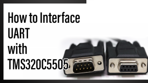
Example 7: UART
Project Description:
This example code shows the character on hyper terminal in pc.
Hardware Connections:
| HARDWARE PIN OUT | CONNECTIONS | OUTPUT | |
| SCIATX | GPIOF4 | Make switch 1 & 2 in SW16 for UART A(SCIA)Make switch 3 & 4 in SW16 for UART B(SCIB) | Output will be displayed in hyper terminal for UART A |
| SCIARX | GPIOF5 | ||
| SCIBTX | GPIOG4 | ||
| SCIBRX | GPIOG5 |
Source Code:
UART on TMS320F2812 Kit
#include "DSP281x_Device.h"

#include  void InitSystem(void);

void SCI_Init(void);

void single_UART(unsigned char cmd);

void UART_conv(unsigned long int conv);

void Delay_1ms(long);

char message[] = {"The F2812-UART is fine !\n\r"};

int index =0;

// pointer into string long i;

void main(void)

{

unsigned long i;

EALLOW;

GpioMuxRegs.GPFMUX.bit.SCIRXDA_GPIOF5 = 1;

// muxing the uart pin GpioMuxRegs.GPFMUX.bit.SCITXDA_GPIOF4 = 1;

EDIS;

InitSystem();

// Initialize the DSP's core Registers SCI_Init();

while(1)

{

SciaRegs.SCITXBUF=message[index++];

while( SciaRegs.SCICTL2.bit.TXEMPTY == 0);

//wait for TX -empty if (index > 26) index =0;

for(i=0;i<150000;i++);

// Software - delay approx. 2 sec.

}

}

void InitSystem(void)

{

EALLOW;

SysCtrlRegs.WDCR= 0x0068;

// Setup the watchdog

// 0x00E8 to disable the Watchdog , Prescaler = 1

// 0x00AF to NOT disable the Watchdog, Prescaler = 64 SysCtrlRegs.SCSR = 0;

// Watchdog generates a RESET SysCtrlRegs.PLLCR.bit.DIV = 10;

// Setup the Clock PLL to multiply by 5 SysCtrlRegs.HISPCP.all = 0x1;

// Setup Highspeed Clock Prescaler to divide by 2 SysCtrlRegs.LOSPCP.all = 0x2;

// Setup Lowspeed CLock Prescaler to divide by 4

// Peripheral clock enables set for the selected peripherals. SysCtrlRegs.PCLKCR.bit.EVAENCLK=0;

SysCtrlRegs.PCLKCR.bit.EVBENCLK=0;

SysCtrlRegs.PCLKCR.bit.SCIAENCLK=1;

SysCtrlRegs.PCLKCR.bit.SCIBENCLK=0;

SysCtrlRegs.PCLKCR.bit.MCBSPENCLK=0;

SysCtrlRegs.PCLKCR.bit.SPIENCLK=0;

SysCtrlRegs.PCLKCR.bit.ECANENCLK=0;

SysCtrlRegs.PCLKCR.bit.ADCENCLK=0; EDIS;

}

void SCI_Init(void)

{

SciaRegs.SCICCR.all =0x0007;

// 1 stop bit,No loopback No parity,8 char bits,async mode, idle-line protocol SciaRegs.SCICTL1.all =0x0003;

//enable TX, RX, internal SCICLK,

// Disable RX ERR, SLEEP, TXWAKE SciaRegs.SCIHBAUD = 405 >> 8 ;

// 9600 Baud ; LSPCLK = 31.25MHz SciaRegs.SCILBAUD = 405 & 0x00FF;

SciaRegs.SCICTL1.all =0x0023;

// Relinquish SCI from Reset

}

void UART_conv(unsigned long int conv)

{

unsigned int j=0,cap_freq1,cap_freq2,cap_freq3,cap_freq4,cap_freq5,cap_freq6;

cap_freq1 = conv/1000;

cap_freq2 = conv%1000;

cap_freq3 = cap_freq2/100;

cap_freq4 = cap_freq2%100;

cap_freq5 = cap_freq4/10;

cap_freq6 = cap_freq4%10;

single_UART(cap_freq1+0x30);

single_UART(cap_freq3+0x30);

single_UART(cap_freq5+0x30);

single_UART(cap_freq6+0x30);

for(j=0;j<1250;j++);

}

void single_UART(unsigned char cmd)

{ SciaRegs.SCITXBUF=cmd;

while ( SciaRegs.SCICTL2.bit.TXEMPTY == 0);

}

void Delay_1ms(long end)

{

long i;

for (i = 0; i <(9000 * end);i++);

}
Verify Output:
These characters are “The F2812-UART is fingvbbbbbbbbbbbbbbbvccv
In the LCD display program why you have used 33H (line 99) and 32H in your program?