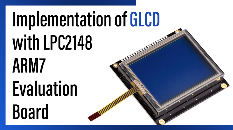
Implementation of GLCD with LPC2148 – ARM7 Evaluation Board
The ARM7 LPC2148 Evaluation Board is specifically designed to help students to master the required skills in the area of embedded systems. The kit is designed in such way that all the possible features of the microcontroller will be easily used by the students. The kit supports in system programming (ISP) which is done through serial port.
NXP’s ARM7 (LPC2148), ARM Evaluation Kit is proposed to smooth the progress of developing and debugging of various designs encompassing of High speed 32-bit Microcontrollers.
GLCD (Graphical Liquid Crystal Display)
The Graphics LCD as the name suggests is a type of LCD which can display graphics. The graphical representation of any data presents good understanding than just characters. More user friendly applications can be designed by using the graphical LCDs.
Interfacing GLCD
Fig. 1 shows how to interface the GLCD to microcontroller. The 128X64 Graphical LCD interfaces to adjust contrast through trim pot. The GLCD needed to create 8-bit interface; 8 data bits (D0 – D7), three control lines, address bit (RS), read/write bit (R/W) and control signal (E), Page Select (CS).
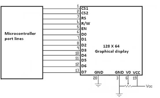
Description of GLCD
The GLCD is divided into two parts which are controlled by two different controllers. Each of these parts is divided into rows and columns.
To interface this GLCD with microcontroller, two registers (Input and Output register) are provided in the LCD. These registers are selected by the combination of RS and RW signals. These combinations are given in the following Table1.
Input Register
Input Register is used while giving instructions and writing data to LCD. It holds the data/instruction temporarily before writing to DDRAM (Data Display RAM).
When the LCD is in active mode (CS1 and CS2 high), the Input register can be selected by sending bits on RS and RW pins as shown in the following table. The data of input register is latched in at the falling edge (from high to low) of EN (Enable) signal and written into DDRAM automatically through internal operation.
Output Register
Output Register is used to read data from DDRAM and to check status data (busy check). When the LCD is in active mode (CS1 and CS2 high), the Output register can be selected by sending bits on RS and RW pins as shown in the following table. When R/W and RS are high, data is latched into output register and when R/W=H, RS=L, status data (busy check) can be read out.
The basic operation with graphical LCD requires following steps
- LCD Initialization
- Page Selection
- Column Selection
- Data Display
All these steps have been explained in the following sections with corresponding instruction sets.
LCD Initialization
Before displaying anything on graphics LCD, it must be initialized, i.e., display must be put on and column/page selection be made. This is achieved by giving proper instructions to the LCD. To make Display On\Off the following set of instructions must be followed in order
- Put these values in Data Register
| DB7 | DB6 | DB5 | DB4 | DB3 | DB2 | DB1 | DB0 |
| 0 | 0 | 1 | 1 | 1 | 1 | 1 | D |
Data appears when D=1 and disappears when D=0. When the display is off, there is no effect on the data which is stored in DDRAM.
- CS1=1, CS2=1(to activate display of both halves of LCD)
- RS=0, R/W=0 (to select the instruction mode)
- EN=1
- Delay
- EN=0 (to latch data into the input register)
Display on/off function can also be used to blink data continuously on the LCD by switching the display with some delay.
Page selection
Before writing any data, the page of LCD must be selected. Page can be selected through following steps
- Put these values in Data Register
| DB7 | DB6 | DB5 | DB4 | DB3 | DB2 | DB1 | DB0 |
| 1 | 0 | 1 | 1 | 1 | X3 | X2 | X1 |
Since there are a total of 8 pages (0–7), a particular page is selected by setting three bits (X1-X3).
- CS1=1, CS2=1(to activate display of both halves of LCD)
- RS=0, R/W=0 (to select the instruction mode)
- EN=1
- Delay
- EN=0 (to latch data into the input register)
For example, if X3=0, X2=1 and X1=0, and then the second page is selected. Reading or writing operation is done on this page until next page is set. Depending on the column selection, the page is selected from either left or right half of the graphics LCD.
Column selection
There are 128 [64 (=26) columns per half] in graphics LCD and they are automatically incremented. This means that after selecting a column, it increases on its own by one, after each write cycle.
So it is easier to write data column by column. A column can be chosen through following instructions
- Put these values in Data Register
| DB7 | DB6 | DB5 | DB4 | DB3 | DB2 | DB1 | DB0 |
| 0 | 1 | Y5 | Y4 | Y3 | Y2 | Y1 | Y0 |
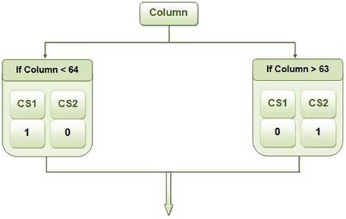
The corresponding controller (CS1 or CS2) is selected depending on the Column number as shown below.
- RS=0, R/W=0 (to select the instruction mode)
- EN=1
- Delay
- EN=0 (to latch data into the input register)
For example, if Page address is 0 and Column address is 0, then 0th column of page 0 is selected, i.e., the first pixel will be selected which is highlighted in the following diagram.
Display data
After page and column selection, data can be sent to LCD for display. The programming steps for display data are as given below
- Put the data values in Data Register. With every write cycle, data is written in one column and the column then gets auto-incremented. A high data bit (DBx = 1) corresponds to activated (dark) pixel and low data bit (DBx = 0) corresponds to deactivated (light) pixel. Here MSB corresponds to 8th row in column and LSB to 1st row of column.
- If column<63 then=”” cs1=”0″ cs2=”1)</li” else=””>
- RS=1 and R/W=0 (to select write mode of LCD)
- EN=1
- Delay
- EN=0 (to latch data into the input register)
If data port is given value ‘0x99’ or ‘10011001’ then column takes the values as shown below.
The following points can be included in above programming steps for efficient programming
- While sending data to be written with array, one can specify the array limit as well. This limit signifies the number of columns one wants to write at once. If the limit is 8, eight columns will be written at once and if it is 7, seven columns will be written in one go.
- The condition ‘if (column >127)’ can be used to return the control back to the main function if the limit exceeds the number of columns present in the LCD.
- The function for setting column should be called again if array limit condition doesn’t fit in left page and has to be extended to right page too.
- Though column address increases itself by one but one variable should be taken to check the conditions (ii) & (iii) explained above.
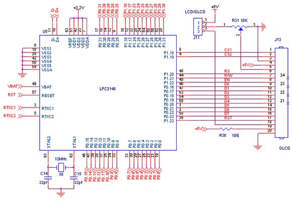
Interfacing GLCD with LPC2148
We now want to display a text in LPC2148 Evaluation Board by using GLCD module. In LPC2148 Evaluation Board contains the LCD and GLCD connections in a single header.
The ARM7 LPC2148 Evaluation Board has numbers of GLCD connections, connected with I/O Port lines (P1.18 – P1.22 && P0.16 – P0.23) to make GLCD display.
Pin Assignment with LPC2148
GLCD/LCD
LCD | 128×64 GLCD Selection
Circuit Diagram to Interface GLCD with LPC2148
Source Code
The Interfacing GLCD with LPC2148 program is very simple and straight forward, which display a text in 128 X 64 GLCD modules. Some delay is occurring when a single command / data is executed.
C Program to display a text in GLCD using LPC2148
***********************************************************************************************************
Title : Program to display data in GLCD usiing LPC2148 – ARM7 Friendly
************************************************************************************************************
#include
#include "Glcd.h"
#include "bmp_maska.h"
#include "Utility.h"
unsigned char
	ii;
char
	*someText;
int main (void)
{
	PINSEL0 = 0;
	PINSEL1 = 0;
	PINSEL2 &= 0x0000000C;
	PINSEL2 |= 0x00000030;
	DelayProc(0.2 * CCLOCK);
	IODIR0 = 0;
	Glcd_Init(&IOPIN0,	// Control lines Port
						&IOPIN0,	// Data Lines Port
						10,				// CS1#
						11,				// CS2#
						12,				// RS
						13,				// R/W#
						15,				// RST
						14,				// EN
						16);			// D0 data line position


	while (1)
	{
		Glcd_Fill(0x00);
		Glcd_Image( maska_bmp );
		DelayProc(2.0 * CCLOCK);
		Glcd_Fill(0x00);
		Glcd_Line(120,1, 5,60, 1);
		Glcd_Line(12,42, 5,60, 1);
		DelayProc(1.0 * CCLOCK);
		Glcd_Rectangle(12,20, 93,57, 1);
		DelayProc(1.0 * CCLOCK);
		Glcd_Line(120,12, 12,60, 1);
		DelayProc(1.0 * CCLOCK);
		Glcd_H_Line(5,15, 6, 1);
		Glcd_Line(0,12, 120,60, 1);
		Glcd_V_Line(7,63, 127, 1);
		DelayProc(1.0 * CCLOCK);
		for (ii = 1; ii <= 10; ii++)
			Glcd_Circle(63,32, 3*ii, 1);
		DelayProc(1.0 * CCLOCK);
		Glcd_Box(12,20, 70,57, 2);
		DelayProc(1.0 * CCLOCK);
		someText = "BIG:ONE";
		Glcd_Write_Text(someText, 5,3, 2);
		DelayProc(1.0 * CCLOCK);
		someText = "SMALL:NOT:SMALLER";
		Glcd_Write_Text(someText, 20,5, 1);
		DelayProc(1.0 * CCLOCK);
	}
}
To compile the above C code you need the KEIL software. They must be properly set up and a project with correct settings must be created in order to compile the code. To compile the above code, the C file must be added to the project.
In Keil, you want to develop or debug the project without any hardware setup. You must compile the code for generating HEX file. In debugging Mode, you want to check the port output without microcontroller Evaluation Board. The Flash Magic software is used to download the hex file into your microcontroller through UART0.
Testing the Graphical LCD Module with LPC2148
Give +3.3V power supply to LPC2148 Evaluation Board; the Graphical LCD is connected with microcontroller LPC2148 Board. When the program is downloading into LPC2148 in Evaluation Board, the screen should show the picture output.
If you not reading any output from Graphical LCD, then you just check the jumper connections & adjust the trim pot level. Otherwise you just check it with debugging mode in Keil. If you want to see more details about debugging just see the videos in below link.
General Information
- For proper working use the components of exact values as shown in Circuit file. Wherever possible use new components.
- Solder everything in a clean way. A major problem arises due to improper soldering, solder jumps and loose joints.
- Use the exact value crystal shown in schematic.
- More instructions are available in following articles,
How to Interface LCD with LPC2148 ARM7 Evaluation Board