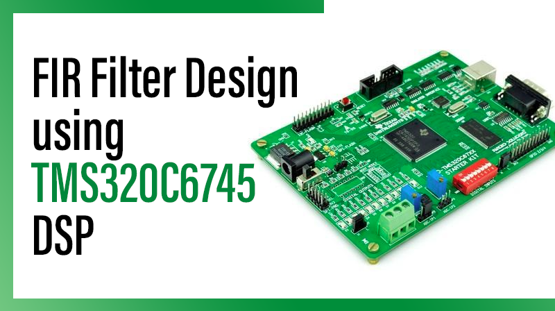
FIR Filter Design using TMS320C6745 DSP
The TMS320C6745 DSP Development Board is specially designed for developers in dsp field as well as beginners. The kit is designed in such way that all the possible features of the DSP will be easily used by everyone.
The kit supports in Code Composer Studio3.3 and later, with XDS100 v1 USB Emulator which is done USB port. This blog post explains about FIR Filter Design using TMS320C6745 DSP.
ADC
An analog-to-digital converter (abbreviated ADC, A/D or A to D) is a device that converts a continuous quantity to a discrete time digital representation. An ADC may also provide an isolated measurement. The reverse operation is performed by a digital-to-analog converter (DAC).
Typically, an ADC is an electronic device that converts an input analog voltage or current to a digital number proportional to the magnitude of the voltage or current.
DAC
A Digital-to-Analog converter (abbreviated DAC, D/A or D to A) is a device that converts a digital value to a continuous analog signal representation. The DAC may also provide an isolated measurement. The reverse operation is performed by an analog to digital converter (ADC).
Typically, a DAC is an electronic device that converts a digital number to an analog voltage proportional to the resolution of bit.
Basic SPI
The ADC and DAC are SPI Bus based which is a serial bus. So the number of pins in IC is very low. Total of four lines are required to interface ADC & DAC it with TMS320C6745.
- MISO (Master In Slave Out)
- MOSI (Master Out Slave In)
- SCK (Serial Clock)
- CS (Chip Select)
As you know in synchronous serial communication there is a clock line (SCK in case of SPI) which synchronizes the transfer.
The clock is always controlled by the MASTER. In our case the TMS320C6745 is the MASTER and the MCP3202 & MCP4921 is a slave on the bus. SPI is full duplex that means data can be sent and received simultaneously.
MCP4921 devices are voltage output string DACs. These devices include input amplifiers, rail-to-rail out-put amplifiers, reference buffers, shut down and reset-management circuitry. The coding of these devices is straight binary.
Digital Output Code
The digital output code produced by an A/D Converter is a function of the input signal and the reference voltage. For the MCP3202, VDD is used as the reference voltage. As the VDD level is reduced, the LSB size is reduced accordingly. The theoretical digital output code produced by the ADC is shown below.
Where:
VIN = analog input voltage
VDD = supply voltage
Analog Voltage Output
The analog voltage output produced by a D/A Converte
r is a function of the input digit and the reference voltage. For the MCP4921, Vref is used as the reference voltage. The theoretical Vout Analog voltage output produced by the D/A Converter is shown below.
Where:
VREF = reference voltage
G = Gain
DN = Input Digits
n = number of bit
FIR FILTER
In signal processing, a finite impulse response (FIR) filter is a filter whose impulse response (or response to any finite length input) is of finite duration, because it settles to zero in finite time.
This is in contrast to infinite impulse response (IIR) filters, which may have internal feedback and may continue to respond indefinitely (usually decaying).
The impulse response of an Nth-order discrete-time FIR filter (i.e., with a Kronecker delta impulse input) lasts for N + 1 samples, and then settles to zero.
The output y of a linear time invariant system is determined by convolving its input signal x with its impulse response b.
For a discrete time FIR filter, the output is a weighted sum of the current and a finite number of previous values of the input. The operation is described by the following equation, which defines the output sequence y[n] in terms of its input sequence x[n]:
Where:
x[n]is the input signal,
y[n]is the output signal,
biare the filter coefficients, also known as tap weights, that make up the impulse response,
N is the filter order; an th-order filter has terms on the right-hand side.
The x[n-i] in these terms are commonly referred to as taps, based on the structure of a tapped delay line that in many implementations or block diagrams provides the delayed inputs to the multiplication operations. One may speak of a 5th order/6-tap filter, for instance.
Note: Practical & Coding explanations are given in this below blog,
Circuit Diagram of SPI ADC & DAC withTMS320C6745

Program to Implement FIR Filter Design using TMS320C6745 DSP
Title : C Porgram To Implement Fir Filter Design Using TMS320C6745
#include

#include

#include "c6745.h"

#include "spiadc.h"

#include "spidac.h"


#define DAC_CS_LOW();   SPI0_SPIPC3 = 0x0;   //(CS=Low:Enable)

#define DAC_CS_HIGH();  SPI0_SPIPC3 = 0x1;   //(CS=High:Disable)


void SPI_Write(unsigned short Data);


unsigned short i,j=0,High,Value=0;

signed int adc_value;


void main( void )

{

       static Uint8 spiadcbuf[3];

       short imp[20];

       int i,xval[50];

       int temp,k,coeff[53]={0},sum;

    coeff[0] = 0x090E;

    coeff[1] =  0x0F45C;

    coeff[2] =  0x04C00;

    coeff[3] =  0x0E4D7;

    coeff[4] =  0x0517C;

    coeff[5] =  0x0517C;

    coeff[6] =  0x0E4D7;

    coeff[7] =  0x0104C;

    coeff[8] =  0x0F45C;

    coeff[9] =  0x090E ;

       C6745_init();

       spiadc_init();

       spidac_init();


       for(i=0;i<52;i++)

       {

               xval[i]=0;

       }

       while(1)

       {

               spiadcbuf[0] = 0x01;    // setup command

               spiadcbuf[1] = 0xBF;

               spiadcbuf[2] = 0x00;

               spiadc_cycle(spiadcbuf, 3);  // Execute spiadc read cycle

               adc_value = ((spiadcbuf[1]&0x0f) << 8)| spiadcbuf[2];

// FILTER FUNCTION

               xval[0] = adc_value;

               sum = 0x0;

           for(k=0;k<10;k++)

           {

                temp = (xval[k])*(coeff[k]);

                sum = sum + temp;

           }

           sum = sum >> 16;

           SPI_Write(sum);

           for(i=8;i>=0;i--)

           {

               xval[i+1] = xval[i];

           }

       }

}


/****************************/

/* GLCD SPI Sent Data 8 bit */

/****************************/

void SPI_Write(unsigned short Data)

{

       unsigned short receive;


       DAC_CS_LOW();

       Data = ( 0x3000 | Data );


       /* Clear any old data */

       receive = SPI0_SPIBUF;


       // Wait for transmit ready

    while( SPI0_SPIBUF & 0x10000000 );


       /* Write 1 byte */

       SPI0_SPIDAT1 = Data;

       while((SPI0_SPIBUF & 0x20000000)==1);


       /* Read 1 byte */

       receive = SPI0_SPIBUF;


       for(j=0;j<10;j++);

    DAC_CS_HIGH();

}