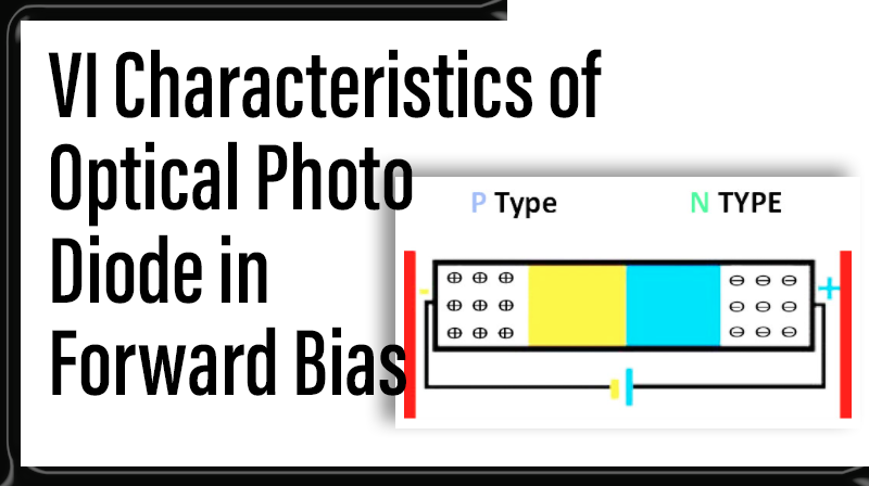
VI Characteristics of Optical Photo Diode in Forward Bias
Aim
To Study the VI Characteristics of Photo Diode in Forward Bias
Apparatus Required
☞Fiber optics Photo diode module – 01
☞Plastic Fiber cable 1 meter – 01
☞Multi meter – 01
☞Adapter +12V/ DC – 01
☞Patch Chords – 04
Theory of VI characteristics of optical photo diode
Principle of Photo Diode
Photodiodes are frequently used photo detectors. They are semiconductor devices which contain a p–n junction, and often an intrinsic (undoped) layer between n and p layers. Devices with an intrinsic layer are called P-I-N or PIN photodiodes. Light absorbed in the depletion region or the intrinsic region generates electron–hole pairs, most of which contribute to a photocurrent. The photocurrent can be quite precisely proportional to the absorbed (or incident) light intensity over a wide range of optical powers.
Operation Modes
Photodiodes can be operated in two very different modes:
1) Photovoltaic mode:
In this process like a solar cell, the illuminated photodiode generates a voltage which can be measured. However, the dependence of this voltage on the light power is nonlinear, and the dynamic range is fairly small. Also, the maximum speed is not achieved.
2) Photoconductive mode:
Here, a reverse voltage is applied to the diode (i.e., a voltage in the direction where the diode is not conducting without incident light) and measures the resulting photocurrent. (It may also suffice to keep the applied voltage close to zero.) The dependence of the photocurrent on the light power can be very linear over six or more orders of magnitude of the light power, e.g. in a range from a few nanowatts to tens of milliwatts for a silicon p–i–n photodiode with an active area of a few mm2. The magnitude of the reverse voltage has nearly no influence on the photocurrent and only a weak influence on the (typically small) dark current (obtained without light), but a higher voltage tends to make the response faster and also increases the heating of the device.
Forward Bias Operation
Procedure
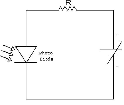
☞Connect +12V adapter Photo Diode module.
☞Measure the series resistance R.
☞Switch (sw1) ON Photo Diode Module and Multi meter.
☞Connect the multi meter probe, positive to P5 and negative to P6 Ground.
☞Now we get a DC voltage output on multi meter and vary the pot meter min to max range (0V to 5V).
☞Connect P5 and P3 test point, P6 and P4 test point using patch chord.
☞Keep pot meter at minimum position.
☞Now vary the pot meter min to max and note down the reading of Resistor across voltage (Vr) and Diode across voltage (Vd).
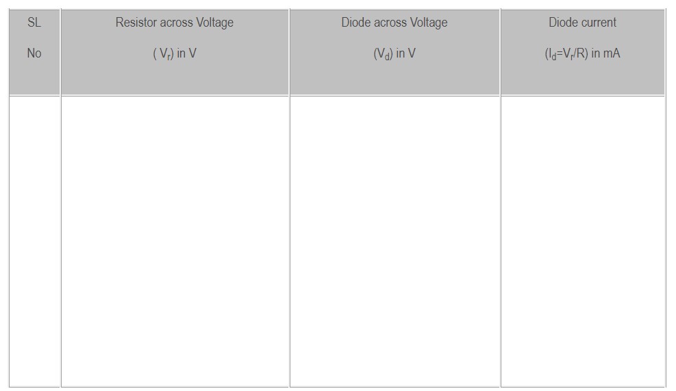
☞Tabulate all the readings in below tabular column.
☞And plate voltage vs current curve.
Tabular column
Series Resistance R = 150Ω
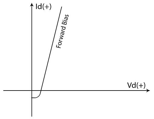
Model Graph
Result
Thus the VI characteristic of Optical Photo Diode in Forward bias was plated.