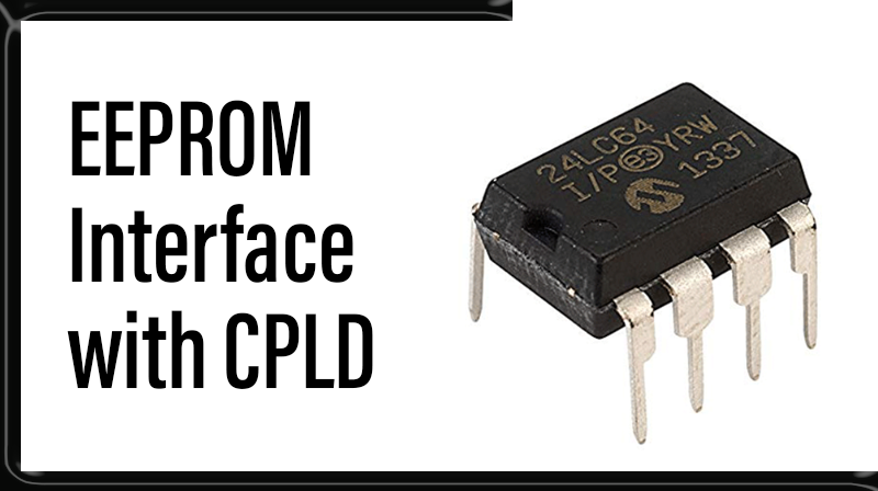
EEPROM Interface with CPLD
EEPROM
The AT24C02A provides 2048 bits of serial electrically erasable and programmable read-only memory (EEPROM) organized as 256 words of 8 bits each. The device is optimized for use in many industrial and commercial applications where low-power and low-voltage operation are essential.
I2C EEPROM Pin Details
SERIAL CLOCK (SCL):
The SCL input is used to positive edge clock data into each EEPROM device and negative edge clock data out of each device.
SERIAL DATA (SDA):
The SDA pin is bidirectional for serial data transfer. This pin is open-drain driven and may be wire-ORed with any number of other open-drain or open collector devices.
DEVICE/PAGE ADDRESSES (A2, A1, A0):
The A2, A1 and A0 pins are device address inputs that are hard wired for the AT24C02. As many as eight 1K/2K devices may be addressed on a single bus system
WRITE PROTECT (WP):
The AT24C01A/02/04/08A/16A has a Write Protect pin that provides hardware data protection. The Write Protect pin allows normal Read/Write operations when connected to ground (GND).
Interfacing EEPROM with CPLD Development Kit
The CPLD Development Kit has I2C EEPROM, indicated as in Figure. The SCL is clock input and is used to synchronize EEPROM with FPGA for various operations. When data is to be read or write, first a start condition is created followed by device address, byte address and the data itself. Finally a stop condition is provided. The start condition occurs when SDA and SCL get high to low simultaneously. The stop condition is when SDA remains low while SCL goes from high to low. The data is read or written between the start and stop conditions on every transition of SCL from high to low.
CLOCK and DATA TRANSITIONS:
The SDA pin is normally pulled high with an external device. Data on the SDA pin may change only during SCL low time periods. Data changes during SCL high periods will indicate a start or stop condition as defined below.
START CONDITION:
A high-to-low transition of SDA with SCL high is a start condition which must precede any other command.
STOP CONDITION:
A low-to-high transition of SDA with SCL high is a stop condition. After a read sequence, the stop command will place the EEPROM in a standby power mode.
ACKNOWLEDGE:
All addresses and data words are serially transmitted to and from the EEPROM in 8-bit words. The EEPROM sends a zero to acknowledge that it has received each word. This happens during the ninth clock cycle.
EEPROM Write Operation
EEPROM Byte Write
A write operation requires an 8-bit data word address following the device address word and acknowledgment. Upon receipt of this address, the EEPROM will again respond with a zero and then clock in the first 8-bit data word. Following receipt of the 8-bit data word, the EEPROM will output a zero and the addressing device, such as a microcontroller, must terminate the write sequence with a stop condition.
EEPROM Page Write
A page write is initiated the same as a byte write, but the FPGA does not send a stop condition after the first data word is clocked in. Instead, after the EEPROM acknowledges receipt of the first data word, the FPGA can transmit up to seven (1K/2K) data words. The EEPROM will respond with a zero after each data word received. The microcontroller must terminate the page write sequence with a stop condition
EEPROM Read Operation
Current Address Read
The internal data word address counter maintains the last address accessed during the last read or write operation, incremented by one.
Sequential Read
Sequential reads are initiated by either a current address read or a random address read. After the microcontroller receives a data word, it responds with an acknowledgement. As long as the EEPROM receives an acknowledgement, it will continue to increment the data word address and serially clock out sequential data words.
VHDL Code Description for EEPROM Write Operation
The EEPROM Write sends device address, word address followed by array of bytes to be stored in the RTC. All this communication happens with START, Acknowledge and STOP bit.
VHDL Code for EEPROM Write Operation
library IEEE;
use IEEE.STD_LOGIC_1164.ALL;
use IEEE.STD_LOGIC_ARITH.ALL;
use IEEE.STD_LOGIC_UNSIGNED.ALL;

entity eeprom_write is
port ( clk : in std_logic;
       reset : in std_logic;
		 sda   : inout std_logic;
		 scl   : inout std_logic;
		 l1    : out std_logic);
end eeprom_write;

architecture Behavioral of eeprom_write is
type state is (start,state1,stop);
signal ps : state := start;
type arr is array(0 to 11) of std_logic_vector(7 downto 0);
constant datas : arr := (x"05",x"00",x"32",x"04",x"32",x"32",x"d2",x"a2",x"04",x"9a",x"f2",x"aa");
signal ack : std_logic := '1';
begin
process(ack,reset,clk)
variable i,j,n : integer := 0;
begin
if reset = '1' then
if clk'event and clk = '1' then

if ps = start then
if i <= 250 then
i := i + 1;
sda <= '1';
scl <= '1';
elsif i > 250 and i < 500 then
i := i + 1;
sda <= '0';
scl <= '1';
elsif i = 500 then
i := 0;
sda <= '0';
scl <= '0';
ps <= state1 ;
end if;
end if;
---------------------------------------------------------------------
if ps = state1 then
if i <= 250 then
i := i + 1;
scl <= '0';
if j < 8 then
sda <= datas(n)(j);
elsif j = 8 then
ack <= sda;
end if;
elsif i > 250 and i <= 500 then
i := i + 1;
scl <= '1';
if j < 8 then
sda <= datas(n)(j);
elsif j = 8 then
ack <= sda;
end if;
elsif i > 500 and i < 520 then
i := i + 1;
scl <= '0';
if j < 8 then
sda <= datas(n)(j);
elsif j = 8 then
ack <= sda;
end if;
elsif i = 520 then
scl <= '0';
i := 0;
if j < 8 then
j := j + 1;
elsif j = 8 then
j := 0;
n := n + 1;
end if;
end if;
if n = 10 then
ps <= stop;
end if;
end if;
if ps = stop then
if i <= 250 then
i := i + 1;
scl <= '1';
sda <= '0';
elsif i > 250 then
i := i + 1;
scl <= '1';
sda <= '1';
end if;
end if;
end if;
if ack = '0' then
l1 <= '0';
elsif ack = '1' then
l1 <= '1';
end if;

end if;
end process;
end Behavioral;