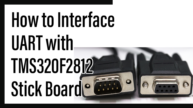
How to Interface UART with TMS320F2812 Stick Board
The Tms320f2812 Evaluation Board is specially desgined for developers in dsp field as well as beginners. The F2812 kit is designed in such way that all the possible features of the DSP will be easily used by the everyone.
The kit supports in Code Composer Studio3.1 and later, with XDS100 v1 USB Emulator which is done USB port.
UART
UART (Universal Asynchronous Receiver Transmitter) are one of the basic interfaces which provide a cost effective simple and reliable communication between one controller to another controller or between a controller and PC.
RS-232 Level Converter
Usually all the digital ICs work on TTL or CMOS voltage levels which cannot be used to communicate over RS-232 protocol. So a voltage or level converter is needed which can convert TTL to RS232 and RS232 to TTL voltage levels. The most commonly used RS-232 level converter is MAX232.
This IC includes charge pump which can generate RS232 voltage levels (-10V and +10V) from 5V power supply. It also includes two receiver and two transmitters and is capable of full-duplex UART/USART communication.
RS-232 communication enables point-to-point data transfer. It is commonly used in data acquisition applications, for the transfer of data between the microcontroller and a PC.
The voltage levels of a microcontroller and PC are not directly compatible with those of RS-232, a level transition buffer such as MAX232 be used.
Interfacing UART
Fig. 1 shows how to interface the UART to microcontroller. To communicate over SCI, UART or USART, we just need three basic signals which are namely, RXD (receive), TXD (transmit), GND (common ground). So to interface UART with TMS320F2812 we just need the basic signals.
Fig. 1 Interfacing UART to Microcontroller
Interfacing UART with TMS320F2812
We now want to display a text in PC from F2812 Evaluation Board by using SCI module. In F2812 Evaluation Board contains two serial interfaces that are SCI A & SCI B. Here we are using SCI A. The Transmitter pins send the data into PC.
Circuit Diagram to Interface UART with TMS320F2812
C Program to Transmit data using TMS320F2812 KIT
Title : Program to Transmit the data to PC from TMS320F2812 kit through SCI A module
#include "DSP281x_Device.h"

// Prototype statements for functions found within this file. void Gpio_select(void);

void InitSystem(void);

void SCI_Init(void);

unsigned int baud_rate=0;

void main(void)

{

char message[]={"The F2812-UART is fine !\n\r"};

int index =0;

// pointer into string long i;

InitSystem();

// Initialize the DSP's core Registers Gpio_select();

// Setup the GPIO Multiplex Registers SCI_Init();

while(1)

{

SciaRegs.SCITXBUF=message[index++];

while ( SciaRegs.SCICTL2.bit.TXEMPTY == 0);

//wait for TX -empty if (index > 26)

{

index =0;

for(i=0;i<150000;i++);

// Software - delay approx. 2 sec.

}

}

}

void Gpio_select(void)

{

EALLOW;

GpioMuxRegs.GPAMUX.all = 0x0;

// all GPIO port Pin's to I/O

GpioMuxRegs.GPBMUX.all = 0x0;

GpioMuxRegs.GPDMUX.all = 0x0;

GpioMuxRegs.GPFMUX.all = 0x0;

GpioMuxRegs.GPFMUX.bit.SCIRXDA_GPIOF5 = 1;

//SCI-RX GpioMuxRegs.GPFMUX.bit.SCITXDA_GPIOF4 = 1;

//SCI-TX GpioMuxRegs.GPEMUX.all = 0x0;

]GpioMuxRegs.GPGMUX.all = 0x0;

GpioMuxRegs.GPADIR.all = 0x0;

// GPIO PORT as input GpioMuxRegs.GPBDIR.all = 0x0;

// GPIO Port B15-B8 input , B7-B0 output GpioMuxRegs.GPDDIR.all = 0x0;

// GPIO PORT as input GpioMuxRegs.GPEDIR.all = 0x0;

// GPIO PORT as input GpioMuxRegs.GPFDIR.all = 0x0;

// GPIO PORT as input GpioMuxRegs.GPGDIR.all = 0x0;

// GPIO PORT as input GpioMuxRegs.GPAQUAL.all = 0x0;

// Set GPIO input qualifier values to zero GpioMuxRegs.GPBQUAL.all = 0x0;

GpioMuxRegs.GPDQUAL.all = 0x0;

GpioMuxRegs.GPEQUAL.all = 0x0;

EDIS;

}

void InitSystem(void)

{

EALLOW;

SysCtrlRegs.WDCR= 0x0068;

// Setup the watchdog

// 0x00E8 to disable the Watchdog , Prescaler = 1

// 0x00AF to NOT disable the Watchdog, Prescaler = 64 SysCtrlRegs.SCSR = 0;

// Watchdog generates a RESET SysCtrlRegs.PLLCR.bit.DIV = 10;

// Setup the Clock PLL to multiply by 5 SysCtrlRegs.HISPCP.all = 0x1;

// Setup Highspeed Clock Prescaler to divide by 2 SysCtrlRegs.LOSPCP.all = 0x2;

// Setup Lowspeed CLock Prescaler to divide by 4

// Peripheral clock enables set for the selected peripherals. SysCtrlRegs.PCLKCR.bit.EVAENCLK=0; SysCtrlRegs.PCLKCR.bit.EVBENCLK=0;

SysCtrlRegs.PCLKCR.bit.SCIAENCLK=1;

SysCtrlRegs.PCLKCR.bit.SCIBENCLK=0;

SysCtrlRegs.PCLKCR.bit.MCBSPENCLK=0;

SysCtrlRegs.PCLKCR.bit.SPIENCLK=0;

SysCtrlRegs.PCLKCR.bit.ECANENCLK=0;

SysCtrlRegs.PCLKCR.bit.ADCENCLK=0;

EDIS;

}

void SCI_Init(void)

{

SciaRegs.SCICCR.all =0x0007;

// 1 stop bit, No loopback

// No parity,8 char bits,

// async mode, idle-line protocol SciaRegs.SCICTL1.all =0x0003;

// enable TX, RX, internal SCICLK,

// Disable RX ERR, SLEEP, TXWAKE SciaRegs.SCIHBAUD = 405 >> 8 ;

// 9600 Baud ;

LSPCLK = 31.25MHz SciaRegs.SCILBAUD = 405 & 0x00FF;

SciaRegs.SCICTL1.all =0x0023;

// Relinquish SCI from Reset

}